In wide-web and multi-lane label production, curing consistency across the web width has a direct influence on print quality, converting stability, and long-term process control. While press speed, irradiance, and wavelength selection are often discussed, LED UV diode spacing remains a less visible but equally critical engineering parameter. Diode spacing determines how ultraviolet energy is distributed laterally, shaping the transverse cure profile seen by inks, coatings, and varnishes.
As label presses evolve toward wider formats and higher productivity, uneven transverse curing becomes more difficult to hide. Variations in cure across the web can result in inconsistent surface hardness, color shifts, differential gloss, and unpredictable die-cutting behavior. Understanding how diode spacing influences these outcomes is essential for engineers, press manufacturers, and converters working with LED UV curing systems.
How LED UV Arrays Generate Transverse Energy Distribution
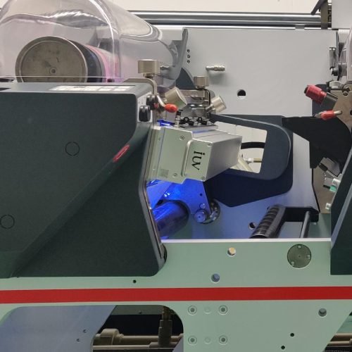
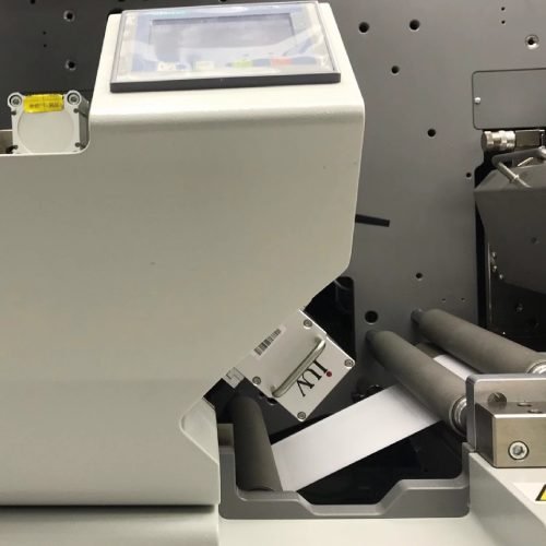
An LED UV curing head is composed of multiple diodes arranged in a linear or modular array. Each diode emits ultraviolet radiation with a defined beam angle and intensity profile. When diodes are positioned at fixed intervals, their individual emission patterns overlap to form a combined irradiance field across the web.
Transverse uniformity depends on how smoothly these emission patterns blend together. If diode spacing is too wide, gaps appear between peak intensity zones, creating low-energy regions across the web. If spacing is too tight, overlapping peaks may produce localized hot spots that accelerate curing in some lanes while stressing substrates in others. The goal is to achieve a balanced overlap that produces a flat and predictable energy profile from edge to edge.
Why Wide-Web Label Formats Increase Sensitivity to Spacing
In narrow web label printing, transverse variations are often masked by short web widths and limited lane counts. As web width increases, small deviations in irradiance become more pronounced and easier to detect. Multi-lane label layouts further amplify the issue, as each lane experiences slightly different curing conditions if the transverse profile is uneven.
Wide-web presses also tend to run higher total output power to maintain curing at speed. This higher power magnifies the impact of diode spacing decisions. Inconsistent spacing that might be acceptable at lower power levels can become problematic when energy density increases, leading to visible differences in ink performance across the web.
Interaction Between Diode Spacing and Optical Geometry
Diode spacing cannot be evaluated in isolation from optical geometry. Lens design, emission angle, and working distance all influence how diode output spreads across the web. A wider beam angle allows greater overlap between diodes, reducing sensitivity to spacing but lowering peak irradiance. A narrower beam concentrates energy but demands tighter spacing to avoid transverse gaps.
Working distance also plays a role. Increasing the distance between the LED UV head and the substrate allows beams to spread and overlap more evenly, but at the cost of reduced intensity. In label printing, where compact press layouts limit working distance, diode spacing must compensate for constrained optical geometry.
Effects on Ink Polymerization Across the Web
UV ink polymerization is highly sensitive to local energy dose. In areas receiving insufficient energy, polymer chains remain underdeveloped, resulting in softer surfaces and potential tack. In overexposed zones, rapid polymerization can increase brittleness, reduce adhesion, or alter gloss.
When diode spacing causes transverse energy variation, these effects appear lane by lane. On wide-web labels, this may show up as uneven scratch resistance, variable rub performance, or inconsistent color density after curing. Such differences complicate quality control and increase the risk of customer rejection.
Influence on Color Consistency and Visual Appearance
Color consistency across the web depends on uniform curing conditions. Even when ink laydown is mechanically consistent, differences in cure rate affect pigment orientation, surface texture, and optical density. Variations in diode spacing that create transverse cure gradients can therefore translate into visible color shifts.
In process color printing, these shifts may be subtle but cumulative. In spot color applications, especially with opaque whites or dense solids, transverse inconsistency becomes more apparent. Maintaining uniform diode spacing helps preserve color fidelity across all lanes and repeat positions.
Mechanical Tolerances and Assembly Accuracy
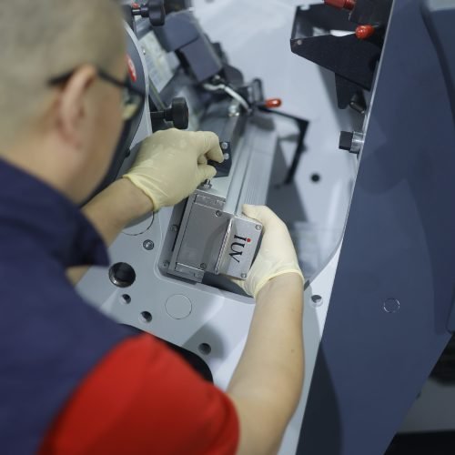
Beyond nominal design spacing, manufacturing and assembly tolerances influence real-world diode placement. Small deviations during assembly can compound across a wide array, altering the intended energy distribution. Thermal expansion during operation can further shift relative diode positions if mechanical support structures are not properly engineered.
High-quality LED UV systems use rigid mounting platforms and controlled assembly processes to maintain consistent spacing under thermal load. For wide-web label presses, these mechanical considerations are critical to sustaining transverse cure uniformity over long production runs.
Edge Effects and Web Margins
Transverse curing challenges are often most severe at the web edges. Diodes near the edges lack symmetrical neighbors, reducing overlap and increasing the risk of undercure. If diode spacing is not adjusted to compensate, edge lanes may consistently receive lower energy than the center of the web.
Engineered solutions include tighter spacing at the edges, modified optics, or dedicated edge compensation zones. These approaches help ensure that labels positioned near the web margins cure to the same standard as those in central lanes.
Relationship Between Diode Spacing and Power Density
Diode spacing directly influences power density distribution. Wider spacing spreads total power over a larger area, reducing local intensity. Tighter spacing increases local intensity but demands precise control to avoid hot spots. In wide-web label production, balancing power density across the web is essential for maintaining both curing performance and substrate safety.
Excessive local intensity may overheat thin films or pressure-sensitive facestocks, while insufficient intensity compromises cure. Proper spacing ensures that power density remains within an optimal range across the entire web width.
Implications for Pinning and Inter-Station Curing
In flexographic presses using LED UV pinning between print stations, transverse consistency is just as important as longitudinal control. Uneven pinning across the web can cause differential ink flow, leading to color shifts or trapping defects in subsequent stations.
Diode spacing that produces uniform transverse energy allows pinning to stabilize ink consistently across all lanes. This uniformity supports sharper image reproduction and improved registration in multi-color label printing.
Thermal Management Considerations
Diode spacing also affects thermal behavior within the LED UV head. Closely packed diodes generate higher localized heat, placing greater demands on cooling systems. Uneven thermal distribution can lead to variations in diode junction temperature, which in turn affect optical output and wavelength stability.
Well-engineered spacing balances optical overlap with thermal dissipation. This balance helps maintain consistent output across the array and reduces long-term degradation differences between diodes positioned at different transverse locations.
Measuring and Evaluating Transverse Cure Uniformity
Assessing the impact of diode spacing requires accurate measurement of transverse irradiance and energy dose. Radiometric mapping across the web provides insight into how evenly energy is distributed. These measurements should be taken under real operating conditions, including production speed and typical power settings.
Print-based evaluations, such as solvent rub tests, surface hardness checks, and die-cut performance comparisons across lanes, complement radiometric data. Together, these methods reveal whether diode spacing achieves the desired curing consistency in practical label production.
Adaptation for Different Label Substrates
Wide-web label presses often process a variety of substrates, from paper to thin films and specialty materials. Each substrate responds differently to curing energy. Diode spacing optimized for one material may not perform equally well for another if transverse energy margins are too narrow.
Systems designed with appropriate spacing flexibility and optical tolerance accommodate these variations more effectively. This adaptability reduces the need for frequent adjustments and supports stable production across diverse label jobs.
Long-Term Performance and Maintenance Impact
Uniform diode spacing contributes to even aging across the LED array. When energy and thermal loads are evenly distributed, diodes degrade at similar rates, preserving transverse uniformity over time. Uneven spacing can cause certain diodes to operate under higher stress, leading to localized output loss and growing cure inconsistencies.
From a maintenance perspective, balanced spacing simplifies performance monitoring and extends useful system life. For converters running wide-web label presses at high utilization, this translates into lower operational risk and more predictable curing behavior.
Engineering Perspective on Diode Spacing Optimization
Optimizing diode spacing is a multidisciplinary task involving optics, thermal management, mechanical design, and process requirements. In wide-web label printing, spacing decisions must consider not only peak output but also how energy is delivered across the entire web under dynamic production conditions.
By treating transverse cure consistency as a primary design objective rather than a secondary outcome, engineers can create LED UV systems that support higher speeds, wider formats, and stricter quality demands. Proper diode spacing remains a foundational element in achieving reliable and repeatable UV curing across wide-web label applications.